The Union government has formulated a comprehensive programme for the development of sustainable semiconductor and display ecosystem.
What are semiconductors?
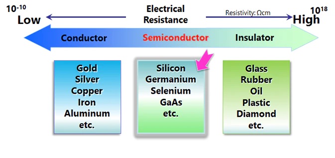
A semiconductor is a material product usually comprised of silicon, which conducts electricity more than an insulator, such as glass, but less than a pure conductor, such as copper or aluminum.
Success in the semiconductor industry depends on creating smaller, faster, and cheaper products.
The bulk of semiconductor manufacturing and supply capability concentrated in a handful of countries including Taiwan, South Korea, U.S., Japan and China.
Types of Semiconductors
Intrinsic semiconductor- It is a pure semiconductor that does not have any impurities or dopants added to it and the number of excited electrons and the number of holes are equal: n = p.
Extrinsic semiconductor- The conductivity of semiconductors can be greatly improved by doping (Adding a small number of suitable substitute atoms known as impurities). It is of 2 types.
N-Type Semiconductor- It is an impurity mixed semiconductor that uses pentavalent impure atoms like phosphorus, arsenic, antimony, bismuth.
Electrons are in the majority and holes are in the minority.
P-type semiconductor- It is a type of extrinsic semiconductor that contains trivalent impurities such as boron and aluminum which increases the level of conductivity of a normal semiconductor made purely of silicon.
Holes are in the majority, and electrons are in the minority.
Other semiconductors
Memory- Memory chips serve as temporary storehouses of data and pass information to and from computer devices' brain
Microprocessors-These are central processing units that contain the basic logic to perform tasks.
Commodity Integrated Circuit-Sometimes called "standard chips", these are produced for routine processing purposes.
Complex SOC-"System on a Chip" is all about the creation of an IC chip with an entire system's capability on it.
What are the properties of semiconductors?
At zero Kelvin, a semiconductor serves as an insulator. It functions as a conductor as the temperature increases.
Semiconductors can be doped to make the semiconductor devices ideal for energy conversion, switches, and amplifiers due to their exceptional electrical properties.
There are fewer power losses.
They have higher resistivity than conductors but a lower resistivity than insulators.
As the temperature increases, the resistance of semiconductor materials decreases, and vice versa.
What is the need for a comprehensive programme for the development of semiconductors?
Semiconductors and displays are the foundation of modern electronics driving the next phase of digital transformation under Industry 4.0.
The chips are now an integral part of contemporary automobiles, household gadgets such as refrigerators, and essential medical devices such as ECG machines.
Semiconductors and display manufacturing is a technology-intensive sector involving huge capital investments, high risk, long gestation and payback periods, and rapid changes in technology, which require significant and sustained investments.
The program will give an impetus to semiconductor and display manufacturing by facilitating capital support and technological collaborations.
It aims to provide attractive incentive support to companies and consortia that are engaged in silicon semiconductor fabs, display fabs, compound semiconductors, silicon photonics, sensors, semiconductor packaging and semiconductor design.
The program will provide a globally competitive incentive package to companies in semiconductors and display manufacturing paving way for India’s technological leadership in the areas of strategic importance and economic self-reliance.
What are the broad incentives have been approved?
Semiconductor Fabs and Display Fabs- This scheme shall extend fiscal support of up to 50% of project cost to eligible applicants.
Government of India will work closely with the State Governments to establish High-Tech Clusters with requisite infrastructure.
Semi-conductor Laboratory (SCL) - The Cabinet has approved that Ministry of Electronics and Information Technology will take requisite steps for modernization and commercialization of SCL.
Compound Semiconductors / Silicon Photonics / Sensors Fabs and Semiconductor ATMP / OSAT Units- This scheme shall extend fiscal support of 30% of capital expenditure to approved units, expecting atleast 15 such units of Compound Semiconductors and Semiconductor Packaging.
Semiconductor Design Companies- The Design Linked Incentive (DLI) Scheme shall extend product design linked incentive of up to 50% of eligible expenditure and product deployment linked incentive of 6% - 4% on net sales for five years.
India Semiconductor Mission: For developing a sustainable semiconductors and display ecosystem, an independent “India Semiconductor Mission (ISM)” will be set up.
ISM will be led by global experts in semiconductor and display industry and it will act as the nodal agency for efficient and smooth implementation of the schemes on Semiconductors and Display ecosystem.
Comprehensive fiscal support for semiconductors and electronics- The Government has approved a programme for development of semiconductors and display manufacturing ecosystem in India with an outlay of Rs.76,000 crore.
Incentive support has been approved under PLI for Large Scale Electronics Manufacturing, PLI for IT Hardware, SPECS Scheme and Modified Electronics Manufacturing Clusters (EMC 2.0) Scheme and for allied sectors.
In total, Government of India has committed support of Rs. 2,30,000 crore to position India as global hub for electronics manufacturing with semiconductors as the foundational building block.
What are the expectations of this move?
Trusted sources of semiconductors and displays hold strategic importance and are key to the security of critical information infrastructure.
The approved program will propel innovation and build domestic capacities to ensure the digital sovereignty of India.
It will also create highly skilled employment opportunities to harness the demographic dividend of the country.
Development of semiconductor and display ecosystem will have a multiplier effect across different sectors of the economy with deeper integration to the global value chain.
The program will promote higher domestic value addition in electronics manufacturing and will contribute significantly to achieving a 1 trillion dollar digital economy and a 5 trillion dollar GDP by 2025.
What are the challenges in this mission?
The level of fiscal support currently envisioned is very less compared to the scale of investments required to set up manufacturing capacities.
India’s PLI scheme intends to give only 50% of the cost of setting up at least two greenfield semiconductor fabs.
Not much of the current scheme outlay is left to support other elements including display fabs, packaging and testing facilities, and chip design centres.
Chip fabs are very thirsty units requiring millions of litres of clean water and extremely stable power supply.