0.1540
900 319 0030
x

Fabrication of Semiconductors

iasparliament Logo
March 28, 2024

Why in news?

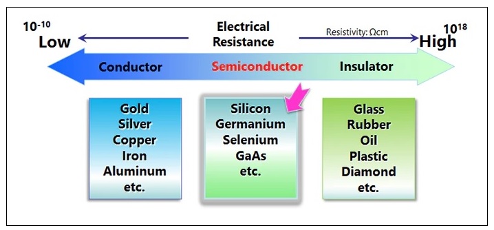
The unique property of semiconductors allows it to control the flow of electric currents.

What is a semiconductor?

  • Semiconductors are materials with electrical properties lying between conductors and insulators.

semiconductor

  • Binary revolution- The digital realm is based on binary language (1s and 0s), which is essential for computing, communication and artificial intelligence, the critical component of this revolution is semiconductor device.
  • Role of semiconductor- They control electric currents with precision and are vital for modern electronics, including smartphones and computers.

Types

  • Intrinsic semiconductor- It is a pure semiconductor that does not have any impurities or dopants added to it and the number of excited electrons and the number of holes are equal: n = p.
  • Extrinsic semiconductor- The conductivity of semiconductors can be greatly improved by doping (i.e., by adding a small number of suitable substitute atoms known as impurities).
    • N-type semiconductor-It is an impurity mixed semiconductor that uses pentavalent impure atoms like phosphorus, arsenic, antimony, bismuth.
    • P-type semiconductor- It is a type of extrinsic semiconductor that contains trivalent impurities such as boron and aluminum which increases the level of conductivity of a normal semiconductor made purely of silicon.
  • Transistor- It is the most important type of semiconductor that enable modern electronics.

Chip 4 initiative includes world’s top semiconductor producing countries namely the U.S., Japan, Taiwan, and South Korea that represents more than 70% of the value of the global semiconductor industry.

How are semiconductors made?

  • Silicon wafer- Silicon sourced from sand, undergoes a meticulous purification process to improve impurities, resulting in an ultra-pure wafer with minimal impurity levels.
  • Photolithography- It involves coating the wafer with a light sensitive material (photoresist), using a mask to imprint the circuit pattern onto the wafer through light.
  • Etching- The engineers use chemical and/or physical techniques to remove the uncarved parts of the photoresist, leaving behind the desired circuit structure on the silicon substrate.
  • Doping- It is a process where impurities are deliberately added to specific parts of the semiconductor to alter its electrical properties, it is done to enable the semiconductors to conduct or block electrical currents as required for its intended function.
  • Deposition- Thin layers of materials such as metals or insulators are deposited onto wafer’s surface, they form electrical connections or insulate components contributing to the functionality of the semiconductor.
  • Testing- The resulting semiconductor product undergoes packaging, where individual chips are separated, encapsulated, and tested to ensure functionality and reliability.
  •  Integration- Finally, the semiconductor chips are integrated into electronic devices, where they contribute to the functionality of the device as a whole.
  • Precision- Fabrication demands ultra-high precision, utilizing scientific principles like photolithography with light sources emitting at 13.5 nm wavelength.

Semiconductor fabrication is the intricate process used to manufacture semiconductor devices.

  • India- It is prominent in chip design, especially in Bengaluru but relies on intellectual property rights owned by parent companies or Arm, limiting its role to that of product user.

What are the benefits of semiconductor?     

  • Employment generation- Semiconductor technology create high-paying jobs, and nurture the potential for deep-tech start-ups.
  • Modern computing- They are critical for the operation of smartphones, laptops, and other computing devices.
  • Connectivity- They are found in routers and switches, crucial for the internet infrastructure that enables global communication.
  • Sustainability- Semiconductors are key in renewable energy technologies like wind turbines and solar panels.
  • Healthcare- They are used in various medical devices, including life-saving implantable devices such as pacemakers and insulin pumps.
  • Automotive- Modern vehicles rely heavily on semiconductors for electronic control systems, security features like remote car keys, safety mechanisms such as anti-lock braking systems, and convenience features like rear-view cameras.
  • Foster innovation- It contributes to advancements in various fields such as materials science, computer engineering, big data, optics, chemical engineering and chip design.

Steps taken by the government to promote the sector

  • Gujarat- It will become the first state in India to have a large-scale semiconductor manufacturing facility.
  • India Semiconductor Mission- It aims to formulate and drive India’s long term strategies for developing semiconductors and display manufacturing facilities and semiconductor design ecosystem.
  • There are 4 subcomponent schemes announced under India Semiconductor Mission.
  • Scheme for setting up of semiconductor fabs in India-It provides fiscal support for setting up semiconductor wafer fabrication facilities in the country.
  • Scheme for setting up of display fabs in India- It provides fiscal support to eligible applicants for setting up of display fabs which is aimed at attracting large investments.
  • Scheme for setting up of Compound Semiconductors / Silicon Photonics / Sensors Fab and Semiconductor Assembly, Testing, Marking and Packaging (ATMP) / OSAT facilities in India - Extends a fiscal support of 50% of the capital expenditure
  • Semicon India Future Design-Design linked incentive (DLI) scheme - Offers financial incentives, design infrastructure support across various stages of development and deployment of semiconductor design.
  • SPECS scheme- It is the scheme for promotion of manufacturing of electronic components and semiconductors and provides financial incentive of 25%.
  • Program for Development of Semiconductors and Display Manufacturing Ecosystem- The modified programme offers fiscal support of 50% of project cost.
  • Semicon India Conclave 2023- India will emerge as global hub of semiconductor and chip-making industry.


References

  1. The Hindu-Explained semiconductor fabrication
  2. PIB- India Semiconductor Mission
Login or Register to Post Comments
There are no reviews yet. Be the first one to review.

ARCHIVES

MONTH/YEARWISE ARCHIVES

Free UPSC Interview Guidance Programme